Return to Section List Return to Menu
= = = 1. LEARN THE DUO COMPACT ARCHITECTURE = = =
The main purpose of the DUO Compact architecture is to interpret machine code instructions and to accommodate I/O devices. DUO Compact machine code is extremely simple. If you haven't already, please learn about the machine code from this page.
= DATA FLOWCHART =
Each block in the diagram represents a group of chips or wires in the DUO Compact:
###########################                       +-------------+
#                         #                       |             |
#   CPU CONTROL SIGNALS   #                       | Peripherals |
#                         #                       |             |
###########################                       +-------------+
       A                                                 A
       |                                                 |
       |                                                 V
+-------------+     +-------------+     #####     +-------------+
|             |     |             |     #   #     |   Mapped    |
|  Microcode  |<----|   NOR ALU   |<---># D #<--->|   Memory    |
|             |     |             |     # A #     |             |
+-------------+     +-------------+     # T #     +-------------+
       A                                # A #            A
       |                                #   #            |
       |                                # B #            |
+-------------+     +-------------+     # U #     +-------------+
| Counter and |     |   General   |     # S #     |   Address   |
| Oscillator  |     |   Memory    |<--->#   #---->|   Latches   |
|             |     |             |     #   #     |             |
+-------------+     +-------------+     #####     +-------------+
Data bus: A bundle of 8 wires attached to many chips in the CPU. The principle is that only ONE chip outputs a value to the bus, while another chip reads the value from the bus. All other chips connected to the data bus MUST have detached outputs, or else there will be a short circuit!
Mapped memory: A composite of several mass storage chips, flip flops, and logic "glue". The mapped memory is addressed by a 16 bit value. The address space is partitioned so that each memory chip has its own dedicated range. EEPROM is granted the largest range: from 0 to 32767. SRAM occupies the next quarter: 32768 to 49151. I/O ports are scattered through the remaining space. Each I/O port is connected to the data bus by a single flip flop.
Address latches: Two 8 bit flip flops. These determine the current address being written or read in mapped memory.
General memory: A small amount of addressable SRAM for scratchwork. The general memory stores intermediate data and the current instruction to execute.
NOR ALU: A set of flip flops, NOR gates, and buffers. This ALU performs the NOR operation for each instruction. It also detects when the NOR result is zero.
CPU control signals: A variety of wires connected to OE pins, WE pins, and (de)multiplexer inputs throughout the machine. This bus commands the CPU to perform simple operations.
Microcode: A pair of EEPROM chips. These output directly to the CPU control signals. The EEPROMs are programmed in such a way that after the contents are read in sequence, the CPU will successfully interpret 1 machine code instruction. Note that the NOR ALU can select one of two sequences in the microcode. This allows the CPU to conditionally skip to one of two addresses in an instruction.
Counter and oscillator: A set of counters and a crystal oscillator. These perpetually count up with a regular tempo. The output value is fed into the microcode EEPROM address so that the microcode may be read in sequence.
= NITTY GRITTY DETAILS =
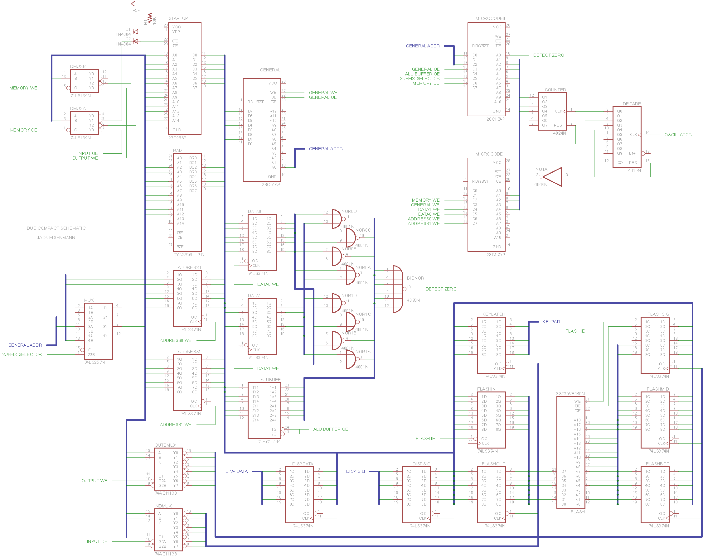
If you are going to build a DUO Compact, you will need a very deep understanding of the architecture! Look at the schematics while reading this section.
These are the sub-components of the mapped memory:
:::::::::::::::     +-------------+     ###############
:   Address   :     |             |     # CPU CONTROL #
:   Latches   :---->| Multiplexer |<----#   SIGNALS   #
:             :     |             |     #             #
:::::::::::::::     +-------------+     ###############
       |                   |                   |
       |                   |                   |
       V                   V                   V
###################################     +-------------+
#                                 #     |             |
#   16 BIT ADDRESS BUS            #---->| Demultiplex |
#                                 #     |     (1)     |
###################################     +-------------+
     |                   |                     |
     |   +---------------|---+-----------------+
     |   |               |   |                 |
     |   |               |   |                 V
     |   |               |   |          +-------------+
     |   |               |   |          |             |
     |   |               +------------->| Demultiplex |
     |   |               |   |          |     (2)     |
     |   |               |   |          +-------------+
     |   |               |   |                 |
     |   |               |   |                 |
     V   V               V   V                 V
+-------------+     +-------------+     +-------------+     +-------------+
|             |     |             |     |             |     |             |
|   EEPROM    |     |    SRAM     |     |  I/O Ports  |<--->| Peripherals |
|             |     |             |     |             |     |             |
+-------------+     +-------------+     +-------------+     +-------------+
       A                   A                   A
       |                   |                   |
       V                   V                   V
#######################################################
#                                                     #
#   8 BIT DATA BUS                                    #
#                                                     #
#######################################################
As you can see from the diagram, the output of the address latches does not feed exclusively into the address bus. The microcode often needs to control the 3 least significant address digits, because each instruction is 8 bytes long (and 2^3 = 8). To control these 3 bits, the microcode uses the multiplexer visible in the diagram. This allows either the address latch output or microcode output to be used as the 3 bottom address bits.
Demultiplexer 1 determines which OE and WE pins will be activated. This demultiplexer only accepts the top 2 most significant address bits, so the chip only controls a single quarter of mapped memory at a time. This degree of precision is sufficient for EEPROM and SRAM (recall that EEPROM occupies 2/4 of mapped memory, and SRAM uses 1/4). I/O ports, on the other hand, occupy individual bytes of mapped memory, so another demultiplexer is necessary.
Demultiplexer 2 activates OE and CP pins for individual I/O ports flip flops. This demultiplexer is activated and deactivated by demultiplexer 1.
The flash chip is a peripheral connected to 5 I/O ports:
###############################################################
#                                                             #
#   8 BIT DATA BUS                                            #
#                                                             #
###############################################################
     |            |            |            A            |
     |            |            |            |            |
     V            V            V            |            V
+---------+  +---------+  +---------+  +---------+  +---------+
| Bottom  |  | Middle  |  | Signals |  |  Data   |  |  Data   |
| Address |  | Address |  |         |  | Output  |  |  Input  |
+---------+  +---------+  +---------+  +---------+  +---------+
     |            |            |            A            |
     |            |            |            |            |
     V            V            V            |            |
+-----------------------------------+       |            |
|                                   |       |            |
|           Flash Memory            |<------+------------+
|                                   |
+-----------------------------------+
Connect your flash chip address pins and control pins as shown below:
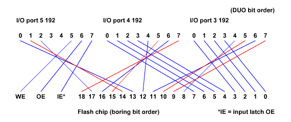
If you fail to use this ordering, DUO OS will not be able to write data to flash.
Use this connection scheme when wiring the screen:
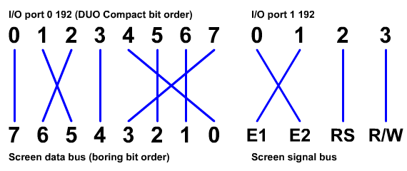
Failing to follow the standard will cause DUO OS to display incorrect characters.
The NOR ALU has a fairly simple layout:
#######################################################     :::::::::::::::
#                                                     #     :             :
#   8 BIT DATA BUS                                    #     :  Microcode  :
#                                                     #     :             :
#######################################################     :::::::::::::::
       |                   |                   A                   A
       |                   |                   |                   |
       V                   V                   |                   |
+-------------+     +-------------+     +-------------+     +-------------+
|    Data     |     |    Data     |     |             |     | Single Big  |
|  Flip Flop  |     |  Flip Flop  |     |   Buffer    |     |  NOR Gate   |
|     (1)     |     |     (2)     |     |             |     |             |
+-------------+     +-------------+     +-------------+     +-------------+
       |                   |                   A                   A
       +-------+   +-------+                   |                   |
               |   |                           |                   |
               V   V                           |                   |
          +-------------+                      |                   |
          |             |                      |                   |
          | 8 NOR Gates |----------------------+-------------------+
          |             |
          +-------------+
The 8 NOR gates each have 2 inputs and 1 output.
The big NOR gate has 8 inputs and 1 output. This NOR gate works in a similar fashion to the standard NOR gate, but will only have a HIGH output if all inputs are LOW.
The composite of microcode EEPROM, counters, and oscillator are shown below:
+-------------+     +-------------+     +-------------+
|             |     |   Decade    |     |   Binary    |
| Oscillator  |---->|   Counter   |---->|   Counter   |
|             |     |             |     |             |
+-------------+     +-------------+     +-------------+
                         |                   |   A
                         |   +---------------+   |
                         |   |               |   |
                         V   V               V   |
                    +-------------+     +-------------+     :::::::::::::::
                    |  Microcode  |     |  Microcode  |     :             :
                    |   EEPROM    |     |   EEPROM    |<----:   NOR ALU   :
                    |     (1)     |     |     (2)     |     :             :
                    +-------------+     +-------------+     :::::::::::::::
                           |                   |
                           |                   |
                           V                   V
                    ###################################
                    #                                 #
                    #   CPU CONTROL SIGNALS           #
                    #                                 #
                    ###################################
The oscillator is a 4 MHz crystal oscillator. It generates a timed signal of HIGH, LOW, HIGH, LOW, etc. For some early tests, you will use a slower oscillator.
The decade counter serves to trigger two actions: increment the binary counter, and pulse the OE of microcode EEPROM 1. These two actions are called perpetually in alternating order.
The binary counter determines the current address for each microcode EEPROM. Note that microcode EEPROM 2 has the ability to reset the binary counter to zero.
Microcode EEPROM 1 sends all WE signals to the CPU. Note that in some cases this output may be demultiplexed.
Microcode EEPROM 2 sends OE and miscellaneous signals to the CPU. One address pin of this EEPROM is controlled by the NOR ALU.
At this point you should be familiar with the purpose of every chip in the DUO Compact. If you have read over this page and you are still confused, contact me at esperantanaso at gmail.com.