Return to Section List Return to Menu
= = = 2. BUILD AND TEST THE BARE CORE = = =
A good convention when building a circuit is to frequently test your work. If you wire two chips incorrectly, the problem will be easier to fix if you find the mistake sooner. The later you procrastinate testing, the more complicated your circuit will be. A more complicated circuit is more difficult to debug.
For this reason I have split the construction of the DUO Compact into manageable pieces. In this section, you will build the bare minimum circuit for interpreting DUO Compact machine code. In the next section, you will add the screen, keypad, and flash memory.
Please note that this construction guide is not 100% granular. I am not going to tell you to "attach a wire from breadboard pin A22 to pin E30". Some important tips:
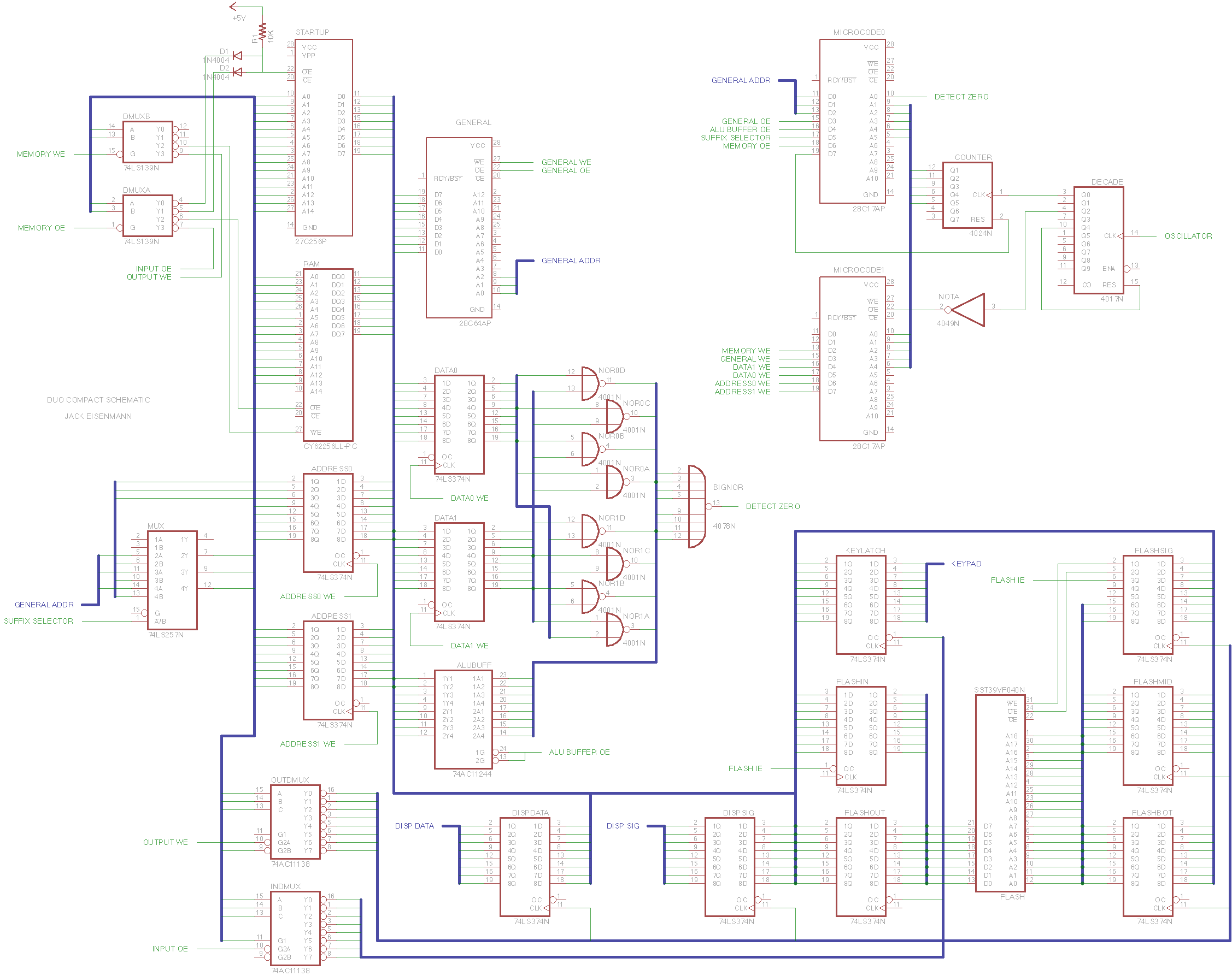
- The DUO Compact schematic is moderately detailed, but you will sometimes need to use rhyme and reason when connecting chips.
- Before using a chip, examine its corresponding data sheet.
- Refer to previous sections of this guide to understand overarching architectural systems.
If you aren't willing to put a little work and thought into this project, turn around now! I don't want you to waste money. If you are up to the challenge, let's begin!
= GET WIRE TOOLS =
For this project, you will use PVC insulated copper wire. You need to strip insulation before plugging any wire into a breadboard. Purchase the tools listed below to facilitate wire stripping:
- Wire cutter
- Wire stripper (preferably with many gauges)
- Needle nose pliers

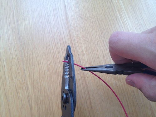
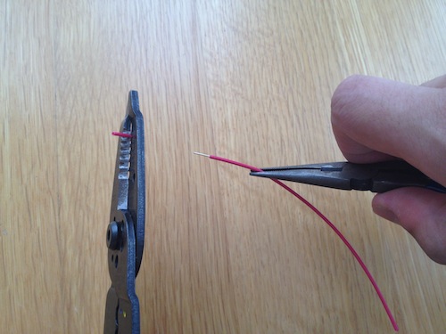
To strip a wire, first use the wire cutter to obtain a wire segment. Next place an end of the wire into the wire stripper. Pull the wire stripper handles firmly together. While holding the handles together, use the needle nose pliers to pull away the rest of the wire. If you succeeded, your wire should have an exposed length of copper.
= BUY THE FIRST ROUND OF COMPONENTS =
Find the list of components on this page. I prefer to use www.mouser.com for most of my electronic parts. Add all of the "first round" components to your cart. Be sure that all quantities are correct. If a particular model of chip is out of stock, find a similar chip with the same part number. Avoid "LS" series chips, since they are not compatible with CMOS technology.
Once you have added the first round parts to your cart, buy them and wait for delivery to complete.
Before you tear open the boxes and bags, beware: CMOS chips are very sensitive to static electricity. A small amount of rogue discharge can kill a chip! Do not handle the chips unless you have recently grounded yourself on a large metal object. Alternatively, use antistatic equipment.
= SET UP A POWER SUPPLY =
If you are unfamiliar with breadboards, please visit this page:
http://eecs.vanderbilt.edu/courses/ee213/Breadboard.htm
Before you plug in chips, you should obtain a reliable 5 volt power supply. I like to find an old USB cable and strip the internal wires. Click the link below to see USB color coding:
Universal Serial Bus Physical Appearance
Connect the power supply to the blue and red strips on the breadboard. Leave the other end of the USB unconnected.
Attach an LED between power strips. LEDs have a positive end and a negative end. Typically the side of the LED with a flat indent should be attached to ground. If your LED does not have an internal resistor, you NEED to put a 500 ohm resistor between the LED and your power supply; otherwise the LED will break!
Now plug the other end of the USB cable into a wall adapter (or laptop port). If you wired the LED correctly, it should turn on! If not, you may have a short circuit; quickly unplug the cable! A short circuit can become hot and melt plastic. Fix any bad wiring before you continue.
= BUILD THE NOR ALU =
The NOR ALU is a good starting point because it contains the simplest chips: flip flops, NOR gates, and buffers.
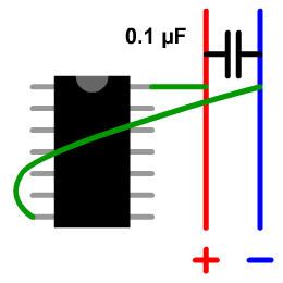
Look at the breadboard layout to see the recommended location for each ALU chip. Turn off the power supply, and plug the chips in! Apply even pressure to all sides of the chips so the pins do not bend. Attach each chip to the power supply column. To make the power supply more steady, add an 0.1 microfarad capacitor between the grounded and sourced pins:
Now wire the chips as specified in the DUO Compact schematic. Try not to mix up the bits as you pass them from chip to chip. Example: Feed the 3rd data bus wire into input 3 of both flip flops. Then feed the output 3 of both flip flops into a single NOR gate. Connect the output of that NOR gate to input 3 of the buffer, and finally connect output 3 of the buffer to the 3rd data bus wire. The 3rd bit should always remain as the 3rd bit!
Next ground each data bus wire with a single 100 kOhm resistor. This will cause each wire to default to LOW unless exposed to a HIGH output.
You have finished your NOR ALU! Before you continue, you must test your circuit. Testing will be especially important if this is your first experience with TTL.
Connect some LEDs to the data bus and to the outputs of the flip flops. (Unless your LEDs have built in resistors, remember to add a resistor between each LED and ground!) Attach the flip flop CP and OE pins to ground, and attach the buffer OE pins to source. You will use these pins to control the flow of data while testing.
Now you can finally power up your ALU! Because the buffer OE is HIGH, the data bus should have all zero bits. Attach some of the data bus wires to source so they become HIGH and their LEDs shine. Next pulse the first flip flop CP pin from LOW to HIGH to LOW. (Connect the CP pin to ground, then to source, then back to ground.) If your circuit is correctly wired, the output of the flip flop will copy the input! If not, turn off the power supply and look at the chip data sheets.
Your arbitrary bit sequence is stored until you disconnect power or write another sequence. Change the data bus bits, and notice that the first flip flop's output will not change. Write the new data bus value into the second flip flop (pulse its CP from LOW to HIGH to LOW).
The first flip flop contains some value "A", while the second flip flop contains some value "B". Disconnect all data bus wires from source. Attach the buffer OE pins to ground. Now the data bus should display the result of A NOR B! If you want, you can write this value back into a flip flop. Alternatively, source the buffer OE again and give one of the flip flops a different value.
The last feature to test is the output of the big NOR gate. Attach an LED to the single output pin, and write 0 to both flip flops. The big NOR gate should have a LOW output. Then set all bits of the first flip flop to 1. The big NOR gate should change its output to HIGH. In essence, the big NOR gate determines whether the outputs of the other 8 NOR gates are all 0.
Perhaps the NOR ALU is not the most exciting circuit, but all DUO Compact instructions use this circuit!
= BUILD THE MAPPED MEMORY =
Now you will construct the mapped memory, which is the largest system in the DUO Compact. I will guide you through some specifics.
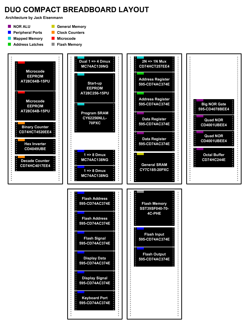
Look at the breadboard layout again and plug in all of the main memory chips. This is also a good time to plug in the address latches, since they are closely tied to the main memory.
Use the schematic to make all necessary connections. Remember to avoid mixing up wires along each path. The following subtleties are not covered in the schematic:
- Any disconnected enable pin should be attached to source or ground so that the chip is always enabled. (See the corresponding data sheet for whether an enable pin should be LOW or HIGH.)
- Disconnected address pins should be grounded. If they are left detached, the chip will access random portions of memory!
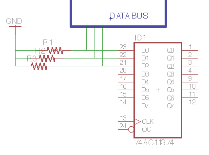
- The output of the multiplexer should be attached to the 3 least significant bits in the address bus. Recall that this mux lets the microcode access each byte in an 8 byte instruction.
- The demultiplexer address determines which quarter of mapped memory to read or write. Attach the most significant address bus bit to the more significant demultiplexer address pin. Attach the second most significant address bus bit to the less significant demultiplexer address pin. If you mix up these address connections, the mapped memory will have incorrect address ranges!
Now power on your machine and try experimenting with the mapped memory. Try to access an address of SRAM by feeding values into the address latches. Change the multiplexer address if necessary. Use the demultiplexers to control the OE and WE pins of SRAM. Write some data into various SRAM addresses (keep OE HIGH and pulse WE HIGH-LOW-HIGH). Check to see that the chip retained the data. As mentioned in a previous section, the SRAM will hold data until you cut off power or write another value. If the chips do not behave as expected, power off the machine and look at their data sheets again.
You are more than half way finished with the DUO Compact core!
= BUILD THE PROCESSOR CLOCK =
The processor clock includes a set of counters, the microcode EEPROMs, and the general memory. After you build the processor clock, your machine will be able to interpret its first instructions.
Plug in the clock chips as shown in the breadboard layout. Before you wire any of the chips, you need to program the microcode chips. Refer to the microcode specification to find the proper data sequence. EEPROM and SRAM chips have similar methods for writing data. To enter a byte into an EEPROM chip:
- Set OE and WE to HIGH, CE to LOW.
- Hard wire each address pin and data pin to the desired value.
- Pulse WE from HIGH to LOW to HIGH.
After you write data to EEPROM, check the values by attaching I/O pins to LEDs and setting OE to LOW.
Now wire the chips according to the schematic. You will need to use long wires for some microcode outputs. The "Oscillator" input will eventually be connected to a 4 MHz oscillator. Remember that if an enable pin has no connection in the schematic, you should hard-wire the pin so the chip will be constantly enabled.
Any microcode output attached to a WE input should either be grounded or sourced with a 100 kOhm resistor. Follow the instructions below.
- Data WE and address WE pins: GROUND with 100 kOhm resistors (default to LOW state).
- Memory WE and general WE pins: SOURCE with 100 kOhm resistors (default to HIGH state).
In order to test the processor clock, you will need a slow source of oscillation. It is possible to use a simple push button, but I don't recommend this. Most push buttons are mechanically imperfect, and can trigger many edge changes in a single press. Instead, you should use the Arduino Uno. Download the Arduino SDK and slow clock program. Upload the program to your Arduino board. Attach pin 0 to an LED and pin 1 to a button. If you hold the button (and the Arduino is powered), the LED should blink on and off.
Connect Arduino pin 0 to the oscillator input of your circuit. If you haven't already, attach LEDs to the microcode outputs. Press and hold the button attached to Arduino pin 1. If you wired the processor clock correctly, the microcode outputs should blink in a hypnotic fashion. Confirm that the output sequence matches the microcode specification.
Before you continue, DISCONNECT any LEDs from the microcode outputs. The LEDs may undo the default states of the 100 kOhm resistors.
= TEST THE CPU CORE =
Right now you have no way to interact with your CPU core. You need a rudimentary form of input and output so that you can test the machine.
Plug in 2 octal flip flops and the 2 remaining demultiplexers to your breadboards. The flip flops will serve as your "debug" input and output ports. The demultiplexers will dictate the port control signals. You must connect each port to the data bus as described below.
- For the debug output port: connect the flip flop input to the data bus, and the output to a set of LEDs.
- For the debug input port: connect the flip flop output to the data bus, and the input to a set of buttons.
Attach the 3 least significant address bus wires to the address pins of the demultiplexers. Connect the 4th least significant address wire to the demultiplexer enable pins (as shown in the schematic). Wire some of the other demultiplexer enable pins to the mapped memory logic glue.
The debug output port must be writable at mapped memory address 600C. The debug input port must be readable at address A00C. Connect the port WE and OE to demultiplexer outputs so that the ports are accessible from the specified addresses. You will need to look at the demultiplexer data sheet and think about binary numbers.
You will use the Arduino to install machine code into your CPU core. Copy the code below and paste it into the DUO Compact emulator:
0000: 00 01 60 0C
4000: 80 00 80 00
8000: FF FB FF FB
C000: 80 00 80 00
0001: 4E 00 00 00
Execute the code and see how it changes the debug output port. Click the "EEPROM ->" convert button and copy the programmer code.
Download the DUO Programmer and find the line which defines const int PROGRAM_DATA_LIST[] PROGMEM". Paste the programmer code from the emulator into the curly braces ({ }). Upload the programmer to your Arduino.
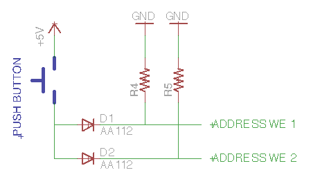
Attach the Arduino pins as described in the programmer comments. Follow the included instructions to install and run the test program. To reset the address registers to zero, trigger the address register WE pins while no data is on the bus. Consider installing a button to perform this action:
For now use the slow clock program as a source of oscillation. After you run the test code, your debug output port should display the value 27 in binary. If this does not occur, add a greater delay to the clock program, and examine data on various buses. This debugging process may be difficult. Some general tips:
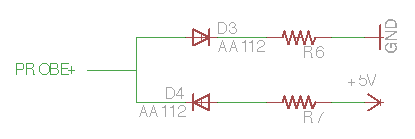
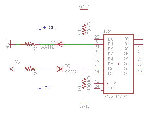
- Remember that each wire may be in a HIGH, LOW, or DETACHED state. If you examine a wire with a single LED, the LOW and DETACHED states may look identical. An input pin with a detached state will behave erratically. Use this probe circuit to recognize all three states:
- Some input pins are vulnerable to ambient fluctuations in charge. If you suspect that a WE pin is being erroneously triggered, attach a 1000 picofarad capacitor between the pin and source. I needed to use such a capacitor for general memory WE.
- The 100 kOhm resistors attached to buses are important. The resistors ensure that if no chip is outputting a value to a bus, the bus will default to a particular state. An LED with a 500 ohm resistor can override the default value set by the 100 kOhm resistor. Be sure that your LEDs do not conflict with the default values:
After the first test program works on your machine, try a second program:
0000: 10 01 00 08
4000: 80 00 80 00
8000: A0 0C 00 08
C000: 01 00 01 00
0100: 00 08 60 0C
4100: 00 00 00 00
0001: 00 FF 00 00
Use the Arduino programmer to install the machine code. Run the code with the slow clock. The program should copy any value from the debug input port to the debug output port. Use the same problem solving techniques if the program does not work as expected.
Lastly, test a third program:
0000: 10 01 00 08
4000: 80 00 80 00
8000: A0 0C 00 08
C000: 01 00 01 00
0100: 20 01 00 08
4100: 02 00 81 00
8100: 30 01 60 0C
C100: 00 00 00 00
0200: 10 01 60 0C
4200: 00 00 00 00
0001: 00 FF F0 EF
The program will write 1 to the debug output port if the debug input port has a value less than 16. Otherwise, the program will write 0. This code will test whether your NOR ALU can detect zero, and whether the processor clock can respond to ALU feedback.
If all of the programs function on your machine, congratulations! You have successfully built the DUO Compact CPU core.